11 Myths About Low-Value Shunt SMD Resistors
What you’ll learn:
While low-ohmic-value resistors may appear alongside standard chip resistors in a typical bill of materials, they present unique challenges at every step of the design and manufacturing process. Debunking these myths will help designers better understand sub-milliohm characteristics and the need for specialist knowledge and techniques.
1. It’s easy to check unmounted resistor values.
In general, resistors are the simplest of components to check prior to mounting. It requires a simple ohmmeter measurement, with 2-terminal connections for higher values and 4-terminal (Kelvin) connections for lower values or higher precision. But resistors with values around 1 mΩ or less require special equipment and great care in fixturing (Fig. 1).
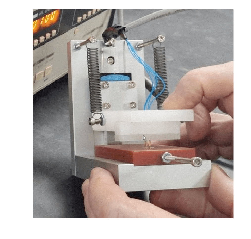
(1) Fixturing is often overlooked. Manual probing doesn’t provide the required accuracy needed. Therefore, a fixture is essential to ensure the probe tips are at the X and Y spacings stated on the datasheet or otherwise advised by the manufacturer.
The measurement system itself needs to be capable of measuring ohmic values in the 100-µΩ to 1-mΩ range with a level of uncertainty that’s small compared to the component tolerance. This may be achieved with a specialist micro-ohmmeter or with a separate programmable current source and millivolt meter. Thermal drift can be an issue, so it’s a good idea to leave the measurement system for at least an hour between switch on and use.
But it’s the fixturing that’s often overlooked. Manual probing will simply not give the accuracy needed. Thus, a fixture is essential to ensure the probe tips are at the X and Y spacings stated on the datasheet or otherwise advised by the manufacturer. The probe contact pattern should be centered on the component—being off-center in either the X- or Y-direction will affect current-flow patterns and hence the ohmic value readings.
The fixture will require maintenance to replace worn probe tips and to ensure no misalignment arises. A repeatability and reproducibility study should be performed to ensure that measurement variation with repeated use and alternative users is acceptable.
2. High-current probe tips are best for the current contacts.
While measurement currents in the region of 5 to 10 A are commonly used, it would seem appropriate to use a high-current sprung probe for the current connections. However, such probes tend to achieve their low contact resistance by having multiple contact points to the termination surface, typically in a circular ring or star shape.
Figure 2A illustrates how such a probe has unpredictable and variable contact locations. They can differ with each application of the probes, giving rise to small but significant variations in the direction of current flow through the component.
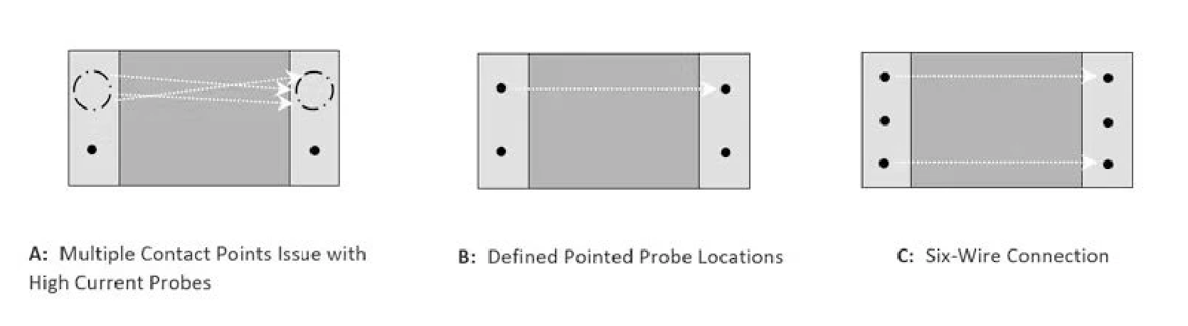
(2) Unpredictable and variable contact locations give rise to small but significant variations in the direction of current flow through the component (A). Single sharp-point probes for the current as well as for the sense contacts set up a precisely defined current flow through the component, and repeatable ohmic value measurements (B). The six-wire arrangement (C) demonstrates two probes used for current connection, creating a symmetrical current-flow pattern closer to that seen in operation on a PCB.
That, in turn, leads to variations in the measured ohmic value. For this reason, it’s advisable to use single sharp-point probes for the current as well as for the sense contacts (Fig. 2B). It will set up a precisely defined current flow through the component, and repeatable ohmic value measurements.
If the current requirements are simply too high to allow for the use of single sharp-point probes, then two probes may be employed for each current connection. This six-wire arrangement (Fig. 2C) has the additional benefit of setting up a symmetrical current-flow pattern closer to that seen in operation on a PCB.
3. It doesn’t matter whether current contacts are directly or diagonally opposite.
The connection format also should be considered; usually, current contacts are on one side of the chip and voltage sense contacts on the other (Fig. 3A). A crossover format (Fig. 3B) may be used, too, and for a given set of location point spacings, it will result in a lower ohmic value reading. This is clear when we consider how the diagonal current flow path may be resolved into a longitudinal and a lateral component (Fig. 3C).
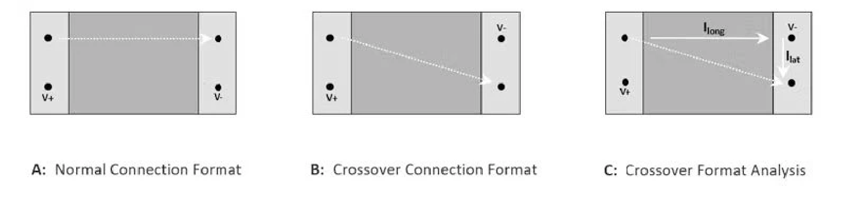
(3) The connection format also should be specified and usually involves current contacts on one side of the chip and voltage sense contacts on the other (A). A crossover format (B) may also be used; for a given set of location point spacings, this will result in a lower ohmic value reading. This becomes clear when we consider how the diagonal current-flow path may be resolved into a longitudinal and a lateral component (C).
The longitudinal component is associated with most of the voltage drop, which is picked up by the sense terminals with the expected polarity. But the lateral component that gives rise to a smaller voltage drop is picked up by the sense terminals with inverted polarity, and therefore reduces the measured value.
4. PCB pad and track design is straightforward.
The PCB layout design around a very-low-value resistor is critical to its performance. The most important aspect of this is the fact that four, rather than two, tracks must be provided to form a Kelvin connection, even when the component itself has only two terminals.
The aim is to minimize the conductive path shared between the current path and the voltage-sensing loop (Fig. 4A), which would increase both the effective ohmic value and the TCR of the mounted part. This may be achieved by connecting the voltage sense tracks to the inner edges of the solder pads (Fig. 4B).
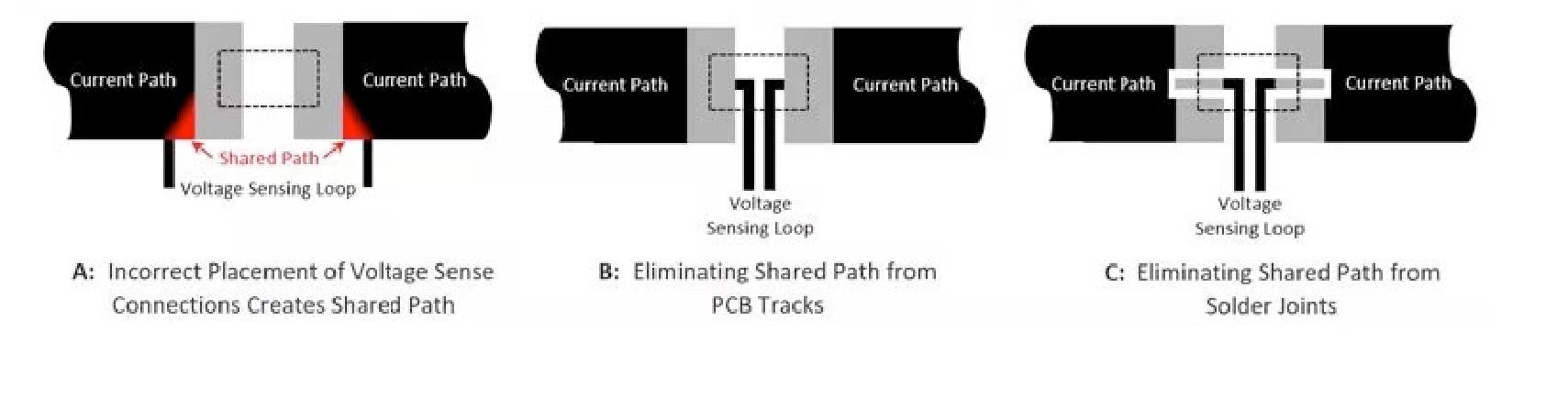
(4) Minimizing the conductive path shared between the current path and the voltage-sensing loop increases both the effective ohmic value and the TCR of the mounted part (A). This may be achieved by connecting the voltage-sense tracks to the inner edges of the solder pads (B). When the voltage-sense pads are split from the current-path pads, the solder joints themselves also are removed from the shared path (C).
You also can take this a step further and split the voltage sense pads from the current path pads, so that the solder joints themselves are also removed from the shared path (Fig. 4C). With this method, it’s possible to approach the accuracy obtained from a true 4-terminal resistor.
Another source of error where high currents are ac or changing dc is due to the voltage-sensing loop linking with changing magnetic fields. This can induce a noise signal superimposed on the desired voltage-sense signal.
To reduce it, the loop area contained within the sense resistor, the two voltage-sense tracks, and the sense circuit input should be minimized. This means keeping the sense circuitry as close as possible to the sense resistor and running the voltage-sense tracks close to each other. A good way to keep these tracks especially close is to superimpose them in different PCB layers.
5. You can easily join shunts in parallel for lower values or higher ratings.
Designers are sometimes forced to use more than one current-sense resistor connected in parallel, either to meet a high power or surge rating, or to achieve an ohmic value lower than the minimum available. This is possible but not easy, and it needs careful layout design. Resistors may be connected in parallel with voltage-sense connections made to just one of the resistors, provided the track layout ensures equal distribution of current between all resistors.
For example, the position in the current trace where the resistors are placed should be well clear of bends or constrictions that could affect the distribution of current density (Fig. 5A). The goal is to ensure that the total track resistance in series with each resistor is the same (Fig. 5B), so that the sensed resistor carries the required fraction of the total current.
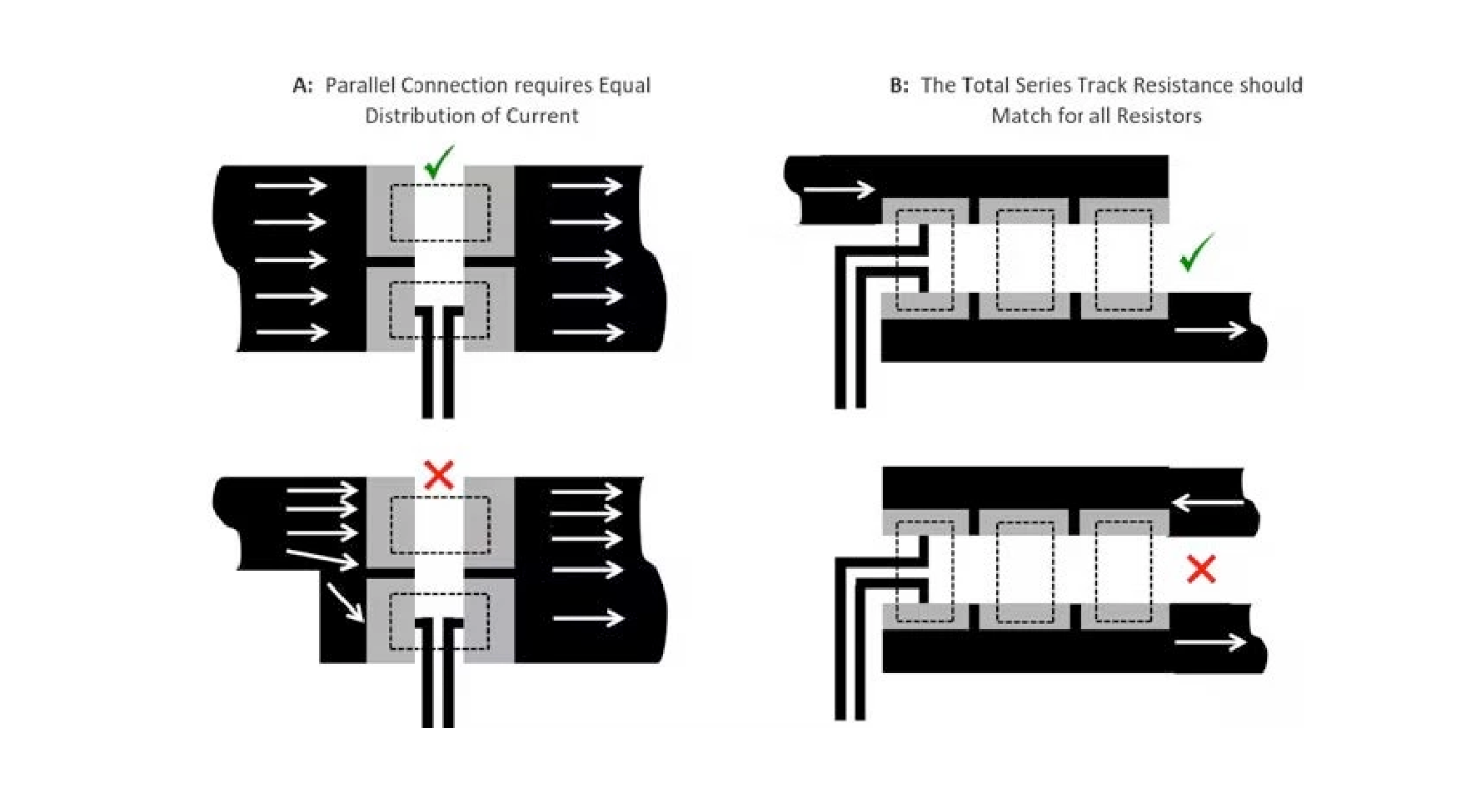
(5) Parallel connection requires equal distribution of current (A). The total series track resistance should match for all resistors (B).
Moreover, it ensures that the proportion of the total current carried by the sensed resistor doesn’t vary with temperature. This would occur with unequal series track resistances due to the high TCR of the copper PCB tracks.
6. The mounted value will equal the unmounted measurement.
The unmounted ohmic value measured in the manner specified by the manufacturer may still be different from the value obtained when the part is mounted on the recommended pad layout. This happens for two reasons.
First, the current flow through the resistor will not be the same when using one or two point contacts at each terminal, as when using a solder joint that connects to most of the lower termination surface. Second, the voltage-sense separation for unmounted measurement needs to be somewhat greater than the minimum theoretically possible, thus allowing for tolerance in the location of probes relative to the resistor. For a mounted part, by contrast, the voltage-sense solder joints will always connect to the innermost points of the termination surfaces.
For these reasons, we can say that two standard methods are able to measure ohmic values of sub-milliohm resistors. The first is to mount the part onto a defined Kelvin connected test PCB, the definitive way to establish ohmic value. The second is to use probed connections, as described previously. In addition, determine a standard mounting offset, normally negative, which is summed with the probe measured value to indicate the predicted mounted value:
Mounting offset = mounted value – probed value
This offset will vary depending on the termination dimensions, which in turn can be a function of the nominal ohmic value. Therefore, it should be regarded as product-specific.
7. The resistance alloy TCR is a good guide to the shunt’s TCR.
The datasheets for low-value shunt resistors may quote two values of TCR. One relates to the resistance alloy TCR and is typically in the ±10- to ±40-ppm/°C range. The other is the actual TCR of the component, taking into account the contribution of the copper terminations.
The two figures are only the same for a true Kelvin shunt in which the current path and voltage-sense loop are separate in the terminations and meet only within the resistance element. Such a construction is relatively costly, so in most cases the actual shunt TCR is greater in magnitude than the resistance alloy TCR. It also depends on the ohmic value, increasing as the value falls.
For example, for 500 µΩ, a shunt TCR in the range ±100 to ±400 ppm/°C is typical, which is 10X greater than the resistance alloy TCR. If a datasheet has only one TCR value, that should be the shunt TCR. When comparing products, it’s clearly important to know which TCR definition applies to which figures.
8. If the layout design is correct, mounting the shunt won’t affect its TCR.
The importance of layout design with correct Kelvin configuration to achieve the minimum TCR has already been described. But the thickness of solder in the finished solder joint also has a direct bearing on both the mounted ohmic value and TCR. That’s because the vertically resolved component of current flow through the solder joint (Fig. 6A) is in a shared path with the voltage-sense loop, which connects at the upper surface of the copper PCB pad. It therefore follows that increased solder thickness (Fig. 6B) will increase the mounted value and associated TCR.
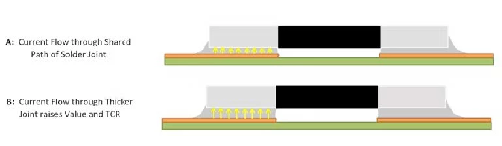
(6) The thickness of solder in the finished solder joint has a direct bearing on the mounted ohmic value. That’s because the vertically resolved component of current flow through the solder joint (A) is in a shared path with the voltage-sense loop, which connects at the upper surface of the copper PCB pad. It therefore follows that increased solder thickness (B) will result in an increase mounted value.
This sensitivity to solder joint thickness can be reduced by using parts with wide area terminations. Such designs aim primarily to lower thermal impedance to the PCB, but reduction in solder thickness sensitivity is an added advantage. Furthermore, the sensitivity also may be eliminated by choosing a 4-termination style shunt. It needn’t be a true Kelvin shunt, because the connection between current path and voltage-sense loop may be made within the termination copper.
9. Shunt temperature rise is just thermal impedance times power.
For a normal resistor, the hotspot temperature rise for a given power dissipation is easily calculated. It’s simply the thermal impedance of the part in °C/W multiplied by the dissipation in W. This can be added to the ambient temperature to give the hotspot absolute temperature.
The situation for very-low-value resistors is more complex because significant dissipation in the shunt implies significant current levels in the PCB tracks. This means that the PCB tracks themselves will contribute to the total temperature rise.
If it’s possible to establish the track temperature rise, then that can be added in to give the actual hotspot temperature. However, if detailed thermal modeling is unavailable, it may need to be determined empirically. But it must be accounted for somehow, otherwise the maximum temperature will be underestimated, with implications for both the thermal design and accuracy calculations.
10. The sensed voltage will be zero if no current is flowing.
Ohm’s law presents an ideal resistor with current in direct proportion to voltage. All resistors deviate from linearity because of finite TCR, but in very low ohmic value parts, the voltage-current curve may not even pass through the origin. A copper terminated-metal-element chip resistor contains at least two boundaries between dissimilar metals. These act as thermocouples and generate a thermoelectric voltage in the presence of a temperature gradient (Fig. 7).
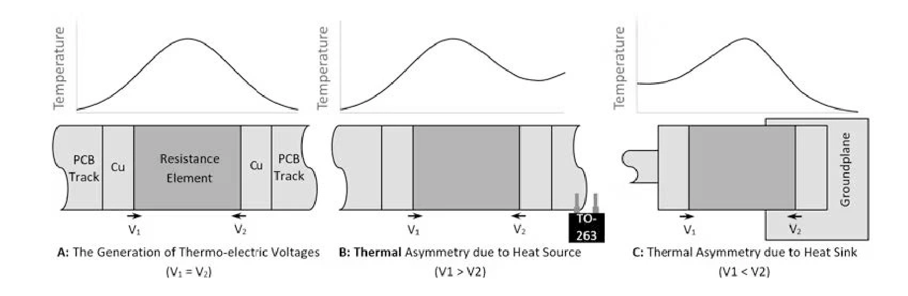
(7) Shown is a balanced state in which the thermal voltages V1 and V2 are equal (A); and an example of imbalance due to the external influence of a heat source and a heat sink (B and C), respectively.
Now these thermocouples are connected in series and, because of the symmetry of the component, are of opposite polarity when the resistor element itself is the main heat source. As a result, if the temperature distribution across the chip resistor is symmetrical, any generated thermoelectric voltages will be cancelled out (Fig. 7A).
However, there may be asymmetry due to the external influence of a heat source (Fig. 7B) or a heat sink (Fig. 7C), respectively. This leads to a finite value of V1 − V2, which sums with the measured sense voltage and creates a source of error. In particular, it may give a false indication of current flow when currents are at or near zero.
11. A low-value SMD shunt is “just another resistor.”
By now, it should be obvious that, although it may be listed alongside standard chip resistors in a bill of materials, a 0.5-mΩ SMD shunt, for example, requires specialist knowledge and techniques at every stage in the design and manufacturing process. This includes component selection, layout design, the inspection of incoming components, and soldering process control.
As a result, it may be advisable to think of low-value SMD shunts as a separate class of component, and expect to invest more time and attention on them with the support of a specialist supplier.