GaN technology presents the power supply industry with opportunities to further refine power conversion, enabling a reduction in the overall size of power supplies.
Silicon-based semiconductors have dominated the electronics industry for more than 70 years. Its cost-effectiveness, abundance, and electrical properties have been well understood, making it the go-to material in the electronics industry. Semiconductor components, such as transistors, integrated circuits (ICs), and diodes, typically use silicon (Si) material in their composition to perform the functions for which they are designed.
In a world dominated by electronics, consumers are increasingly seeking smaller and lighter devices. Power supplies are no different and are typically the largest ‘component’ in any system. Power density is a topic of ongoing discussion, as designers strive to pack the most power into the smallest possible footprint. Gallium Nitride (GaN) technology presents the power supply industry with opportunities to further refine power conversion, enabling a reduction in the overall size of power supplies.
What is GaN?
GaN is a wide-bandgap semiconductor material, meaning it has approximately a 3x larger energy gap between its valence and conduction bands compared to traditional Si. Historically, it has not been as cost-effective or widely available as Si; however, in recent years, it has reached a competitive price point, particularly in lower-power applications. Moreover, compared to Si-based components, GaN offers superior electron mobility and thermal characteristics, making a perfect recipe for optimal efficiency and opening new opportunities in the electronics industry, particularly in the switch-mode power supply (SMPS) sector.
In the world of power conversion, GaN is not a new technology. Its first applications date back to the 1970s, when it was doped with magnesium to create the first LEDs capable of emitting blue light. In the early 2000s, high electron mobility transistors (HEMTs) employing GaN were introduced for radio frequency (RF) applications. GaN technology is, however, a relatively new entrant to the low-power AC-DC industry, driven by increased availability and, consequently, a reduction in material cost in larger volumes. In the 2010s, GaN-based field-effect transistors (FETs) became more widely available for the consumer market, particularly for higher-wattage applications.
But what benefits does GaN technology bring to power supply designs?
Key Benefits of using GaN
At a top level, SMPSs use FETs as fast-switching devices to deliver power to loads efficiently. FET switching is governed by gate-driving ICs that respond to changes in loads through a control circuit that monitors the output of the power supply. Although traditional Si-based metal-oxide semiconductor field-effect transistors (MOSFETs) are commonly used in SMPS applications, significant losses remain in these designs. The main contributors to these losses are conduction, switching, and reverse recovery. With its superior electron mobility and thermal characteristics, GaN technology presents new opportunities for engineers to increase the efficiency of their power supply designs while reducing the overall size.
Conduction Losses
GaN FETs operate similarly to MOSFETs. However, their thermal characteristics and high electron mobility path allow these losses to be minimized. One of the most notable characteristics of a GaN FET is its significantly lower drain-to-source resistance (RDS(on)). When the FET is in saturation mode, power is dissipated as heat. The following equation characterizes this relationship:
So, with GaN FETs, less power is lost as heat when they are in saturation mode. As a side note, conduction losses of a GaN device are like those of a bipolar junction transistor (BJT) device.
Switching Losses
Power losses are also a result of the FET switching process. These losses are due to the input capacitance (Ciss) and the amount of electrical charge required to switch a FET on and off, which is also known as the gate charge (Qg), as well as the voltage between the gate and source terminals (VGS). The following formula relates these parameters:
When the gate of the FET is charged and discharged, switching power losses (Psw) occur in the form of heat. The formula can approximate this:
GaN FETs feature less input capacitance and, therefore, less gate charge. The high switching frequency (fsw) reduces switching losses, contributing to better overall efficiency (see Figure 1).
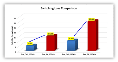
Figure 1: 400V/15A GS66508T and C3M0065090J Switching Loss Comparison
Reverse Recovery Losses
GaN FETs have zero reverse recovery losses. In an Si-based MOSFET, reverse recovery losses occur due to the body diode located at the P- or N-channel junction. The losses are generated when the MOSFET transitions from forward bias (conducting) to reverse bias (non-conducting). This is a parasitic characteristic of every diode that is a result of stored charge in the diode between states. As GaN FETs have no body diode, these losses are eliminated.
Overall, GaN offers the best of both MOSFET and BJT technologies, combining the ease of drive of a MOSFET with the low conduction losses of a BJT. The result is higher operating efficiency, which reduces power losses in the power supply.
Footprint Reduction
Not only do the material properties of GaN allow the FET to be smaller than an Si-based FET, but with less power losses, fewer heat dissipation techniques are required. This means that power supply designers can save even more space with smaller heat-sinking components, contributing further to a smaller footprint.
In addition, the faster fsw of the GaN-based FET allows for traditionally larger passive components, such as transformers and inductors, typically used in Si-based FETs, to be reduced in size. This size reduction also contributes to reducing the overall footprint of the SMPS.
The TT Electronics TEAM and TEAD GaN families of AC desktop power adapters deliver power ranging from 45W to 420W, with a focus on high power density (Figure 2). These new power adapters are 30% lighter and 40% smaller than the company’s existing ITE and medical-certified desktop PEAM and PEAD families. This reduction in size and weight, made possible by using GaN technology, enables a sleek profile that meets the needs of the medical and industrial electronics industries.
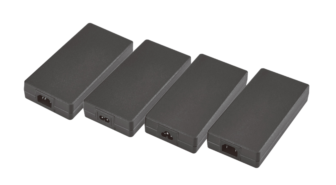
Figure 2: TTE TEAD360 Series
Partner with an Expert
GaN technology has emerged as a transformative force in power supply design, offering numerous benefits over traditional silicon-based semiconductors. With its superior electron mobility, thermal characteristics, and ability to operate at higher frequencies, GaN enables engineers to create power supplies that are not only more efficient but also significantly smaller in size.
The key advantages of GaN, such as reduced conduction, switching, and reverse recovery losses, translate into tangible improvements in power supply performance. These improvements include higher operating efficiency, which in turn leads to less robust heat dissipation requirements. Consequently, this allows for a reduction in the size of passive components, culminating in a more compact power supply footprint.
The TT Electronics TEAM and TEAD GaN families exemplify the practical application of GaN technology, showcasing how it can lead to the development of lighter and smaller power adapters without compromising power output. As GaN technology continues to mature and become more cost-effective, it is poised to revolutionize the power supply industry, meeting the ever-growing demand for more efficient, space-saving electronic devices.
The first step to optimizing power conversion in your next design is to partner with a power supply expert. The TT Electronics engineering team at its power supplies engineering center in Boston MA can work with you, as an extension of your engineering team, to identify and deploy the ideal power supply solution. TT Electronics has a long history of working with OEM partners to achieve the specification required for the application, through power supply modification and customization.
Contact our team today to learn about a complimentary load characterization study – a valuable way to ensure the system meets the power supply requirements, rather than the other way around.